- 您现在的位置:买卖IC网 > Sheet目录509 > SI3853DV-T1-GE3 (Vishay Siliconix)MOSFET P-CH 20V 1.6A 6-TSOP
�� �
�
�Si3853DV�
�Vishay� Siliconix�
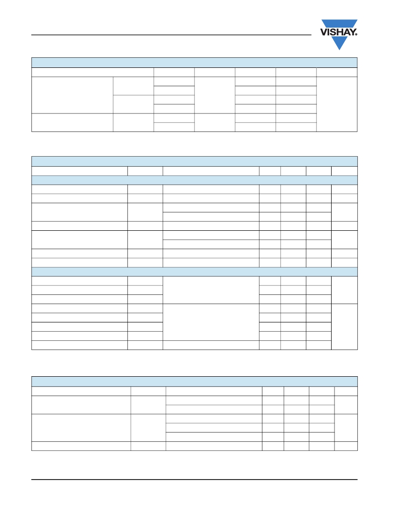
�THERMAL� RESISTANCE� RATINGS�
�Parameter�
�Device�
�Symbol�
�Typical�
�Maximum�
�Unit�
�Junction-to-Ambient� a�
�Junction-to-Foot�
�t� ≤� 5s�
�Steady� State�
�Steady� State�
�MOSFET�
�Schottky�
�MOSFET�
�Schottky�
�MOSFET�
�MOSFET�
�R� thJA�
�R� thJF�
�93�
�103�
�130�
�140�
�75�
�80�
�110�
�125�
�150�
�165�
�90�
�95�
�°C/W�
�Notes:�
�a.� Surface� mounted� on� 1"� x� 1"� FR4� board.�
�MOSFET� SPECIFICATIONS� T� J� =� 25� °C,� unless� otherwise� noted�
�Parameter�
�Symbol�
�Test� Conditions�
�Min.�
�Typ.�
�Max.�
�Unit�
�Static�
�Gate� Threshold� Voltage�
�Gate-Body� Leakage�
�Zero� Gate� Voltage� Drain� Current�
�On-State� Drain� Current� a�
�V� GS(th)�
�I� GSS�
�I� DSS�
�I� D(on)�
�V� DS� =� V� GS� ,� I� D� =� -� 250� μA�
�V� DS� =� 0� V,� V� GS� =� ±� 12� V�
�V� DS� =� -� 16� V,� V� GS� =� 0� V�
�V� DS� =� -� 16� V,� V� GS� =� 0� V,� T� J� =� 75� °C�
�V� DS� ≥� -� 5� V,� V� GS� =� -� 4.5� V�
�-� 0.5�
�-5�
�±� 100�
�-1�
�-� 10�
�V�
�nA�
�μA�
�A�
�Drain-Source� On-State� Resistance� a�
�Forward� Transconductance� a�
�R� DS(on)�
�g� fs�
�V� GS� =� -� 4.5� V,� I� D� =� -� 1.8� A�
�V� GS� =� -� 2.5� V,� I� D� =� -� 1.0� A�
�V� DS� =� -� 5� V,� I� D� =� -� 1.8� A�
�0.160�
�0.280�
�3.6�
�0.200�
�0.340�
�Ω�
�S�
�Diode� Forward�
�Voltage� a�
�V� SD�
�I� S� =� -� 1.05� V,� V� GS� =� 0� V�
�-� 0.83�
�-� 1.10�
�V�
�Dynamic� b�
�Total� Gate� Charge�
�Q� g�
�2.7�
�4.0�
�Gate-Source� Charge�
�Gate-Drain� Charge�
�Turn-On� Delay� Time�
�Q� gs�
�Q� gd�
�t� d(on)�
�V� DS� =� -� 10� V,� V� GS� =� -� 4.5� V,� I� D� =� -� 1.8� A�
�0.4�
�0.6�
�11�
�17�
�nC�
�Rise� Time�
�Turn-Off� DelayTime�
�Fall� Time�
�Body� Diode� Reverse� Recovery� Time�
�t� r�
�t� d(off)�
�t� f�
�t� rr�
�V� DD� =� -� 10� V,� R� L� =� 10� Ω�
�I� D� ?� -� 1� A,� V� GEN� =� -� 4.5� V,� R� g� =� 6� Ω�
�I� F� =� -� 1.05� A,� dI/dt� =� 100� A/μs�
�34�
�19�
�24�
�20�
�50�
�30�
�36�
�40�
�ns�
�Notes:�
�a.� Pulse� test;� pulse� width� ≤� 300� μs,� duty� cycle� ≤� 2� %.�
�b.� Guaranteed� by� design,� not� subject� to� production� testing.�
�SCHOTTKY� SPECIFICATIONS� T� J� =� 25� °C,� unless� otherwise� noted�
�Parameter�
�Forward� Voltage� Drop�
�Symbol�
�V� F�
�Test� Conditions�
�I� F� =� 0.5� A�
�I� F� =� 0.5� A,� T� J� =� 125� °C�
�Min.�
�Typ.�
�0.42�
�0.33�
�Max.�
�0.48�
�0.4�
�Unit�
�V�
�V� R� =� 20� V�
�0.002�
�0.100�
�Maximum� Reverse� Leakage� Current�
�I� rm�
�V� R� =� 20� V,� T� J� =� 75� °C�
�0.06�
�1�
�mA�
�V� R� =� 20� V,� T� J� =� 125� °C�
�1.5�
�10�
�Junction� Capacitance�
�C� T�
�V� R� =� 10� V�
�31�
�pF�
�Stresses� beyond� those� listed� under� “Absolute� Maximum� Ratings”� may� cause� permanent� damage� to� the� device.� These� are� stress� ratings� only,� and� functional� operation�
�of� the� device� at� these� or� any� other� conditions� beyond� those� indicated� in� the� operational� sections� of� the� specifications� is� not� implied.� Exposure� to� absolute� maximum�
�rating� conditions� for� extended� periods� may� affect� device� reliability.�
�www.vishay.com�
�2�
�Document� Number:� 70979�
�S09-2276-Rev.� B,� 02-Nov-09�
�发布紧急采购,3分钟左右您将得到回复。
相关PDF资料
SI3867DV-T1-GE3
MOSFET P-CH 20V 3.9A 6-TSOP
SI3905DV-T1-GE3
MOSFET P-CH D-S 8V 6-TSOP
SI3909DV-T1-GE3
MOSFET 2P-CH 20V 6TSOP
SI3911DV-T1-GE3
MOSFET P-CH DUAL 20V 6TSOP
SI3981DV-T1-GE3
MOSFET P-CH DUAL 20V 6-TSOP
SI3983DV-T1-GE3
MOSFET P-CH DUAL 20V 6-TSOP
SI4056DY-T1-GE3
MOSFET N-CH 100V D-S 8SOIC
SI4100DY-T1-E3
MOSFET N-CH D-S 100V 8-SOIC
相关代理商/技术参数
SI3861
制造商:FAIRCHILD 制造商全称:Fairchild Semiconductor 功能描述:Integrated Load Switch
SI3861BDV
制造商:VISHAY 制造商全称:Vishay Siliconix 功能描述:Load Switch with Level-Shift
SI3861BDV-T1-E3
功能描述:电源开关 IC - 配电 20V 2.3A 0.83W RoHS:否 制造商:Exar 输出端数量:1 开启电阻(最大值):85 mOhms 开启时间(最大值):400 us 关闭时间(最大值):20 us 工作电源电压:3.2 V to 6.5 V 电源电流(最大值): 最大工作温度:+ 85 C 安装风格:SMD/SMT 封装 / 箱体:SOT-23-5
SI3861BDV-T1-GE3
功能描述:模拟开关 IC 20V 2.3A 0.83W 145mohm @ 4.5V RoHS:否 制造商:Texas Instruments 开关数量:2 开关配置:SPDT 开启电阻(最大值):0.1 Ohms 切换电压(最大): 开启时间(最大值): 关闭时间(最大值): 工作电源电压:2.7 V to 4.5 V 最大工作温度:+ 85 C 安装风格:SMD/SMT 封装 / 箱体:DSBGA-16
SI3861DV
功能描述:MOSFET 25/8V/20/8V NCh/PCh Load Switch
RoHS:否 制造商:STMicroelectronics 晶体管极性:N-Channel 汲极/源极击穿电压:650 V 闸/源击穿电压:25 V 漏极连续电流:130 A 电阻汲极/源极 RDS(导通):0.014 Ohms 配置:Single 最大工作温度: 安装风格:Through Hole 封装 / 箱体:Max247 封装:Tube
SI3861DV-T1
功能描述:电源开关 IC - 配电 20V 2.3A 0.83W RoHS:否 制造商:Exar 输出端数量:1 开启电阻(最大值):85 mOhms 开启时间(最大值):400 us 关闭时间(最大值):20 us 工作电源电压:3.2 V to 6.5 V 电源电流(最大值): 最大工作温度:+ 85 C 安装风格:SMD/SMT 封装 / 箱体:SOT-23-5
SI3861DV-T1-E3
功能描述:电源开关 IC - 配电 20V 2.3A 0.83W RoHS:否 制造商:Exar 输出端数量:1 开启电阻(最大值):85 mOhms 开启时间(最大值):400 us 关闭时间(最大值):20 us 工作电源电压:3.2 V to 6.5 V 电源电流(最大值): 最大工作温度:+ 85 C 安装风格:SMD/SMT 封装 / 箱体:SOT-23-5
SI3861DV-T3
制造商:Vishay Siliconix 功能描述:TRANS MOSFET N/P-CH 20V 2.3A 6TSOP - Tape and Reel